(China (Mainland))

Product Summary
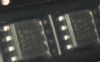
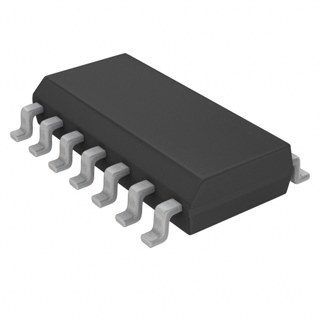
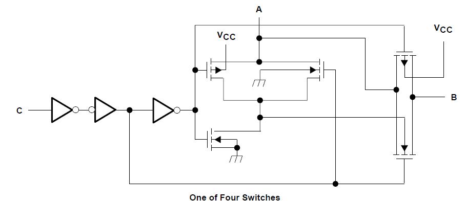
The SN74HC4066DR is a silicon-gate CMOS quadruple analog switch designed to handle both analog and digital signals. Each switch permits signals with amplitudes of up to 6 V (peak) to be transmitted in either direction. The SN74HC4066DR has its own enable input control (C). A high-level voltage applied to C turns on the associated switch section. Applications include signal gating, chopping, modulation or demodulation (modem), and signal multiplexing for analog-to-digital and digital-to-analog conversion systems.
Parametrics
SN74HC4066DR absolute maximum ratings: (1)Supply voltage range, VCC: -0.5 V to 7 V; (2)Control-input diode current, II (VI < 0 or VI > VCC): ±20 mA; (3)I/O port diode current, II (VI < 0 or VI/O > VCC): ±20 mA; (4)On-state switch current (VI/O = 0 to VCC): ±25 mA; (5)Continuous current through VCC or GND: ±50 mA; (6)Package thermal impedance, θJA (see Note 2): D package: 86℃/W; DB package: 96℃/W; N package: 80℃/W; NS package: 76℃/W; PW package: 113℃/W; (7)Storage temperature range, Tstg: -65℃ to 150℃.
Features
SN74HC4066DR features: (1)Wide Operating Voltage Range of 2 V to 6 V; (2)Typical Switch Enable Time of 18 ns; (3)Low Power Consumption, 20-μA Max ICC; (4)Low Input Current of 1 μA Max; (5)High Degree of Linearity; (6)High On-Off Output-Voltage Ratio; (7)Low Crosstalk Between Switches; (8)Low On-State Impedance, 50-Ω TYP at VCC = 6 V; (9)Individual Switch Controls.
Diagrams
| Image | Part No | Mfg | Description |  |
Pricing (USD) |
Quantity | ||||||||||||
|---|---|---|---|---|---|---|---|---|---|---|---|---|---|---|---|---|---|---|
 |
 SN74HC4066DR |
Texas Instruments |
Analog Switch ICs Quadruple Bilateral Analog Switches |
Data Sheet |
|
|
||||||||||||
|
SN74HC4066DRE4 |
Texas Instruments |
Analog Switch ICs Quadruple Bilateral Analog Switches |
Data Sheet |
|
|
||||||||||||
|
SN74HC4066DRG4 |
Texas Instruments |
Analog Switch ICs Quadruple Bilateral Analog Switches |
Data Sheet |
|
|
||||||||||||